![]()
![]()
![]()
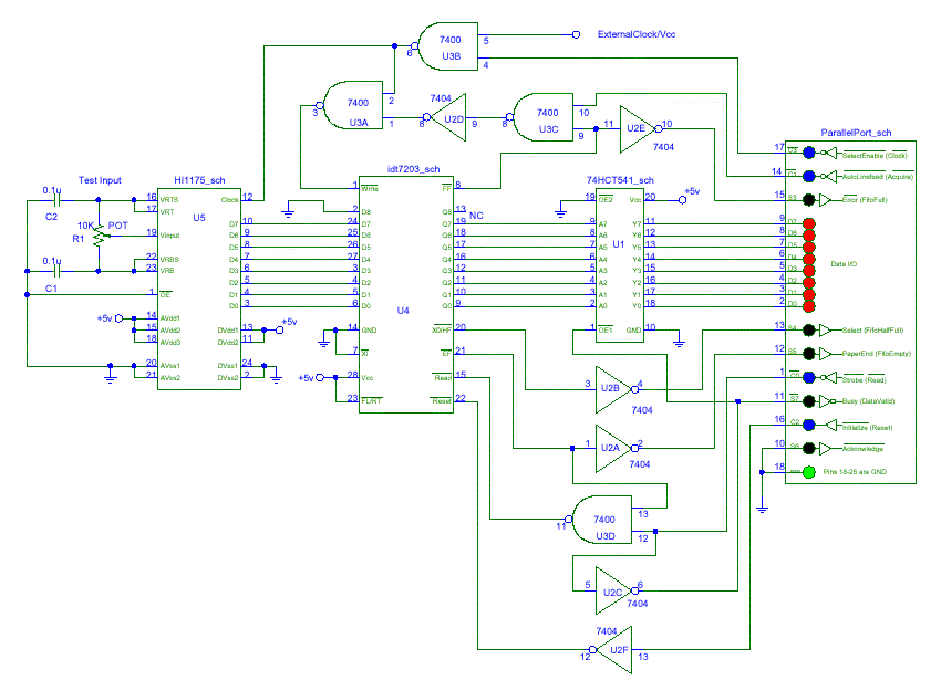
Basic Idea: input signal -> ADC -> FIFO -> ParallelPort -> Computer
I got the original idea for this off the web a few years ago from this site: http://www.ucl.ac.uk/~ucapwas/scope20m.html. My "phase 1" design is very similiar to this. I've added a buffer between the FIFO and the parallel port and the ability to generate a clock via the parallel port or an external clock chip. I'm also using different chips.
You may notice that I've added four 390 Ohm resistors and
LED's... These are to view some of the control signals.
![]()
Circuit Diagram:
 (click on thumbnail for larger image)
![]()
Click here for the PDF version
![]() Click here for the original Pspice
version (you will have to go to www.orcad.com
and download the student version of Pspice and you will need this
symbol library file that I made)
Click here for the original Pspice
version (you will have to go to www.orcad.com
and download the student version of Pspice and you will need this
symbol library file that I made)
![]()
Layout:
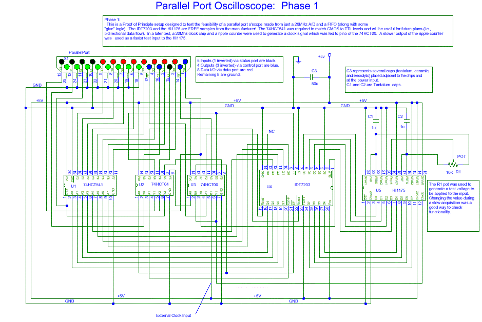 (click on thumbnail for larger image)
![]()
<Click here for the PDF version
Click here for the original Pspice
version (you will have to go to www.orcad.com
and download the student version of Pspice and you will need this
symbol library file that I made)
![]()
Photo of working board:
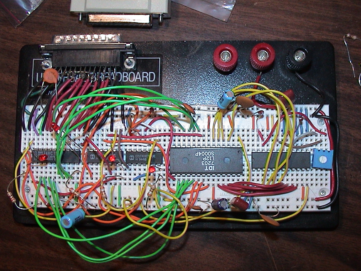 (click on thumbnail for larger image)
 ![]()
Click here for my VBDOS source code. If
you don't know what VBDOS is, it is an old DOS based version of Visual
Basic. It is easy to access the parallel port with this
program. You can also use C to do the same thing. From
windows, things are a little more complicated... If you don't know
what DOS or C or Visual Basic are, you can still open the file with a
text editor and see what I was doing...
![]()
Notes:
![]()
You will need a bi-directional parallel port, because we want to input
data. This may require changing the settings in CMOS setup from ECP/EPP
to bi-directional.
Pull-up resistor, 330p caps, and/or ferrite beads may be required on
the "read" control signal out of the parallel port to prevent
spontaneous FIFO reads.
![]() After some experimenting and investigation, I've found that the HCT
version of the logic chips (7400 and 7404) are the best. These are
fast enough to work at 20MHz and can work with both CMOS and TTL levels.
After some experimenting and investigation, I've found that the HCT
version of the logic chips (7400 and 7404) are the best. These are
fast enough to work at 20MHz and can work with both CMOS and TTL levels.![]() I've gotten a lot of chips for free (beside the ADC and FIFO used
here) and you can too. Many chipmakers let you request samples
right off the web...
I've gotten a lot of chips for free (beside the ADC and FIFO used
here) and you can too. Many chipmakers let you request samples
right off the web... ![]() The Phase 2 plan is to add a timebase using a 20MHz clock chip and a
ripple counter (I've done this already, but I want to make it selectable
via the parallel port), a second input channel (I'll use some logic so
that the one FIFO alternately gets a data point from each of the two
ADC's), an input amplifier (hopefully just one opamp, will need -5VDC?
via a voltage inverter? in order to see signals that drop below 0V,
tricky to get it to work at 20MHz?), and a trigger circuit (maybe just a
comparator and some logic?). Want to add a register to control as
much of this as possible from the parallel port (this will probably
require a bi-directional parallel port [standard]).
The Phase 2 plan is to add a timebase using a 20MHz clock chip and a
ripple counter (I've done this already, but I want to make it selectable
via the parallel port), a second input channel (I'll use some logic so
that the one FIFO alternately gets a data point from each of the two
ADC's), an input amplifier (hopefully just one opamp, will need -5VDC?
via a voltage inverter? in order to see signals that drop below 0V,
tricky to get it to work at 20MHz?), and a trigger circuit (maybe just a
comparator and some logic?). Want to add a register to control as
much of this as possible from the parallel port (this will probably
require a bi-directional parallel port [standard]).